Investigation of Pad Cratering in Large Flip-Chip BGA using Acoustic Emission
$ 11.00 · 4.8 (541) · In stock

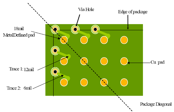
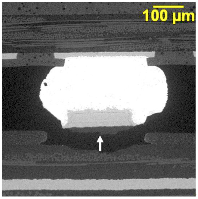
Electronics assemblies with large flip-chip BGA packages can be prone to either pad cratering or brittle intermetallic (IMC) failures under excessive PCB bending. Pad cratering cracks are not detected by electrical testing or non-destructive inspection methods, yet they pose a long term reliability risk since the cracks may propagate under subsequent loads to cause electrical failure. Since the initiation of pad cratering does not result in an instantaneous electrical signature, detecting the onset of this failure has been challenging. An acoustic emission methodology was recently developed by the authors to detect the onset of pad cratering [1, 2]. The instantaneous release of elastic energy associated with the initiation of an internal crack, i.e., Acoustic Emission (AE), can be monitored to accurately determine the onset of both pad cratering and brittle intermetallic (IMC) failures. In this study, the AE technique is used to systematically investigate pad cratering in a daisy chain 40 x 40 mm Flip-Chip BGA (FCBGA) package with lead-free SAC305 solder balls and 1 mm ball pitch. AE sensors have been attached to a fourpoint bend test vehicle to determine the onset of either pad cratering or brittle IMC failures. A two-dimensional AE source location method has been used to determine the planar location of failures on the test board. The test matrix is designed to investigate the effects of normal or diagonal strain orientation, NSMD or SMD PCB pads, and single or multiple reflow cycles. Physical failure analysis has been performed to correlate the test results with failure modes. Introduction Pad cratering refers to the formation of fine cohesive cracks under BGA pads in organic substrates or PCB laminate materials (Figure 1). These cracks have been known to occur under excessive mechanical bending or shock loads that may be applied in PCBA assembly, test, and handling operations [3-6]. Studies have also shown that pad cratering can occur under high thermal strains such as those experienced during SMT reflow processing, thermal cycling with a wide temperature range or thermal shock conditions [7]. The concern for pad cratering has been elevated with the increased use of large body size FCBGA components and fine pitch pad geometries. Furthermore, in comparison with the conventional tin-lead solder alloys, studies have shown that the risk for pad cratering is higher in lead-free assemblies. This is because the stress concentration under BGA pads is higher with the use of the significantly stiffer and more brittle Sn-Ag-Cu (SAC) based alloys, and also due to the use of higher reflow temperatures in assembly [4]. In addition, the Phenolic cured laminate materials compatible with lead-free assembly are more brittle than Dicy cured laminates used in conventional tin-lead assembly processes [8]. Figure 1 Schematic Depiction of Pad Cratering In recent years the industry has made significant advances in developing test methodologies to improve our understanding of pad cratering. A pad level pull test method has been developed to characterize the propensity of different laminate materials and pad designs [8]. This method has now been adopted as IPC standard 9708. However, in addition to pad level tests, board level tests are necessary to develop strain limits for PCBA level test and handling operations. For board level testing, the industry has traditionally relied on performing 4-point bend tests or spherical bend tests, and failure is often defined as the loss of electrical continuity in a daisy chain test vehicle [9, 10]. However in the case of pad cratering, this approach is flawed because the initiation of fine pad cratering cracks does not immediately disrupt the electrical continuity of a daisy chain net. Electrical monitoring of daisy chain nets can only detect a very late stage of pad crater formation when the internal cracks have grown sufficiently large to cause an electrical trace to rupture. In order to circumvent this problem the present authors have recently developed and validated a novel approach which uses acoustic emission to detect the initiation of pad cratering failure [1, 2]. The acoustic emission (AE) approach is unique because it does not rely on an electrical signature to detect the onset of failure; instead elastic stress waves generated by the sudden initiation of pad cratering cracks are detected by piezoelectric sensors mounted on the test board. Our recent studies showed that by detecting AE events during 4-point bend tests we were able to accurately detect the initiation of both pad cratering and brittle intermetallic (IMC) fracture of solder joints [1, 2]. In addition to detecting the onset of failure, with the use of two AE sensors and prior knowledge of the velocity of sound in the PCB laminate, it was possible to accurately determine the location of failures which generated the AE events detected during bend tests. This methodology was validated by showing that the AE events detected during bend test were originating from the edges of the BGA package, which is where the first pad cratering failures would occur. In addition, physical failure analysis validated that solder joint cross-sections from samples without any AE activity did not have any pad cratering, while cross-sections of samples that generated AE events had clear evidence of pad cratering. Using this approach, we were able to determine the PCB strain limits for the initiation of pad cratering failures, and these strain limits were found to be significantly lower than those derived from electrical failure of the daisy chain nets. In this study, the AE method has been applied on a large body size flip-chip BGA (FCBGA) test vehicle to assess the strain limit for pad cratering. In a further extension of the AE methodology, four sensors have been used to determine the planar location of failures generated during four-point bend tests. The effects of design and process variables such as NSMD or SMD pad design, normal or diagonal strain orientation, and single or multiple reflow cycles have been investigated. Test Vehicle The tests were performed on daisy chain 40 x 40 mm FCBGA packages with organic built-up substrate and fully populated Sn-3.0%Ag-0.5%Cu (SAC305) solder balls with 1 mm pitch (Figure 2). The test board was designed to be double sided with the FCBGA assembled either on side A or side B. On side A, the FCBGA was oriented at a 0° angle as shown in Figure 3, while on side B the FCBGA was oriented at a 45° angle as shown in Figure 4. Figure 2 FCBGA Footprint, 40 x 40 mm Body Size, 1mm Pitch The 40 x 40 daisy chain package was tested with either 0° orientation, where the component edges were parallel to the board’s edges or with 45° orientation where the component was at a 45° angle. The 0° board represents the case where the bending axis is normal to the edges of the component, while the 45° board represents the case where the bending axis is along the component diagonals. Arguably the 45° orientation may be more representative of actual handling operations in functional PCB assemblies. In addition to component orientation, the test boards were designed to have either a full array of non-solder mask defined (NSMD) pads, or solder mask defined (SMD) pads at only the six corner-most BGA pads at all four corners of the package. The pad diameter for NSMD PCB pads was the same as the mask opening of the BGA substrate. In the case of SMD pads at package corners, the pad diameter was slightly larger and the solder mask opening matched the mask opening of the BGA substrate. In order to simulate a functional PCB board design, it was desirable to have Plated Through-Hole (PTH) vias connected to all BGA pads. Since this was not possible at the pad locations where side A and side B of the BGA footprint overlapped, only the package corners were designed to be connected to PTH vias. Figure 5 shows the PCB pad layout near the package corners with SMD pads at the six corner-most locations. Note that the PTH vias were located inwards, towards the center of the package, in order to prevent PTH vias from shielding the solder joints during the bend tests. Figure 3 Test Vehicle Side A, 0° Orientation Figure 4 Test Vehicle Side B, 45° Orientation

Investigation of Pad Cratering in Large Flip-Chip BGA using Acoustic Emission
BGA Solder Joint Failure (pad cratering) on RoHS PC – F.O.M.
BGA Pad Cratering - SEM Lab Inc.
![]()
Transient Solder Separation of BGA Solder Joint During Second Reflow Cycle

Figure 3 from Failure mechanism and mitigation of PCB pad cratering

Pad Cratering: Prevention, Mitigation and Detection Strategies

A new detection method for the onset of PCB pad cratering

iST's AE Test Method to Prevent PCB Material from Pad Cratering

Investigation of Pad Cratering in Large Flip-Chip BGA using Acoustic Emission

asys aes 01 - SMT Electronics Manufacturing

A New Approach for Early Detection of PCB Pad Cratering Failures

SMT, PCB, EMS Technical Articles

Investigation of Pad Cratering in Large Flip-Chip BGA using Acoustic Emission

Investigation of Pad Cratering in Large Flip-Chip BGA using Acoustic Emission